4/28/2013

Microcontroller Advanced Kit - MIDI Controller 6N137


This project shows you how the hardware of a MIDI interface works and goes through some simple examples to show how the controller can be used in MIDI systems. First we will start by explaining the details of the hardware interface. Then we will look at the MIDI protocol and see how simple it is to write custom software for this MIDI controller.

There are only a couple parts needed to build the MIDI connections. A few resistors, a diode, and a small 8 pin IC and that is it. The controller part of the system is a 2051 microcontroller (a 20 pin version of the popular 8051). The MIDI interface connects to the serial port of the 2051 (pins 2 and 3). The 2051 also has a reset circuit (the 10 uF capacitor and the 8.2k resistor) and an oscillator circuit (the 24 MHz crystal and the two 33 pF capacitors). For more information on the 2051, The only thing not shown is the 5 volt power supply that creates Vcc (5 Volts DC) for the circuit. An LM7805 and 220 uF capacitor is included with the kit to create 5 Volts DC from a 9 to 12 Volt DC source.


The 6N137 isolates one electrical system from another. There is no electrical connection between devices connected by MIDI. When a current flows through the internal LED connected between pins 2 and 3, the LED transmits light to a light detecting diode. The diode is activated and the Output at pin 6 is pulled low by the internal transistor. If no current flows then the Output floats. Rather than let it float, we connect an 8.2k resistor to pin 6 to lightly pull the voltage at the Output to 5 Volts when the circuit in not active.


The microcontroller sends signals through the MIDI port by controlling the voltage at its pin 3. The current is provided by the 5 volts (Vcc) connected to pin 4 of the MIDI Out port. When the MIDI Out port is connected to a MIDI In port of another system the following circuit is created.


AD8016ARB TMS320F2812PGFA     PCF8584T  SN75176BP PCM1801U
PCI9080-3 MAX211ECAI MAX708CSA MAX1922ESA LM339D
MAX3185CWP LM2903N  MC34119P IR2110       LM2575T-5.0
IR2153       MAX1617MEE        MAX813LCSA MAX797CSE LM358D


4/27/2013

MAX3243CAI RS-232 Transceiver IC Maxim


The MAX3243CAI is a 1μA Supply-Current, True +3V to +5.5V RS-232 Transceiver with AutoShutdown. The MAX3243CAI achieves 1μA supply current with Maxim revolutionary AutoShutdown feature. When the MAX3243CAI does not sense a valid signal level on its receiver inputs, the on-board power supply and drivers shut down. This occurs if the RS-232 cable is disconnected or if the transmitters of the connected peripheral are turned off. The applications of the MAX3243CAI include Notebook, Subnotebook, and Palmtop Computers, Battery-Powered Equipment, Hand-Held Equipment, Peripherals and Printers.


MC34118DW IR2112S L6219DS MAX706CSA ADM202EARN AD826AR EPM7128SLC84-15
ATMEGA8L-8AU AD9883AKST-110 EPM3032ATC44-10 AD9884AKS-140 DG412DY FDS4435
SP3243ECA SAA7111AHZ SAA7118E MAX1644EAE IR2101S LM317 LF347N


4/26/2013

Power Supply Module, AC/DC in, 5V out, Based on 7805 IC L7805CV


Power Supply Board Based on L7805CV IC Design, AC or DC Input, Output DC 5V / 1.5 Amp.
Thermal Overload Protection ( IC Function ).
Short Circuit Protection ( IC Function ).
Output Transition SOA Protection ( IC Function )
Thickness 1.6mm FR-4 Fiber Glass PCB.
HQ Terminal Blocks, Easy Connection Wire.
400V 2Amp Bridge Rectifier 2W04.
2 PCS RUBYCON 1000uF/35V 105℃ HQ Electrolytic Capacitors.
100nF/100V Metal Film Capacitor, Conducive to Filtering High-Frequency Noise.
Output Voltage LED Indicator.
35 x 35 x 12.5 mm Heat-sink.

The item include PCB and parts on PCB, Has passed electrical testing.

Specifications:
AC Input : 6V - 22V ( Transformer No-load Voltage must be less than 22V )
DC Input : 8V - 30V
Output Voltage : DC 5V
Maximum Current : 1.5 Amp ( If Drop-Out or Output Power Very High, Must Increase the Heat-sink  )
PCB Size : 50 x 50mm ( 2 x 2 inch )
PCB Thickness : 1.6mm ( 0.063 inch )
Maximum Height : 37mm ( 1.46 inch )


TEA2025B TLP521-4 SG3524N   NE556N   RTL8019AS NE555N        SAA7113H        PCF8563T  MT8870DS LM393DR
MAX485CPA LM358P       MAX202ECSE MAX238CWG MAX707CSA
AD8052AR AD1885JST EPM7128AETC100-10 BAT54S ADC0809CCN


4/25/2013

LM358N - DEW Sensor


                                  LM358N

The following schematic shows a simple DEW sensor circuit diagram using LM258N IC. As the humidity around the circuit goes up, the resistance in the DEW sensor increases. When the resistance reaches a pre-specified level, the circuitry displays a warning message, and shuts down the external device


Under normal conditions, resistance of the dew sensor is low (1 kilo-ohm or so) and thus the voltage at its non-inverting terminal (pin 3) is low compared to that at its inverting input (pin 2) terminal. The corresponding output of the comparator (at pin 1) is accordingly low and thus nothing happens in the circuit. When humidity exceeds 80 per cent, the sensor resistance increases rapidly. As a result, the non-inverting pin becomes more positive than the inverting pin. This pushes up the output of IC1 to a high level. As a consequence, the LED inside the opto-coupler is energised. At the same time LED1 provides a visual indication. The opto-coupler can be suitably interfaced to any electronic device for switching purpose. Circuit comprising diode D2, resistors R5 and R6 and capacitor C1 forms a low-voltage, low-current power supply unit. This simple arrangement obviates the requirement for a bulky and expensive step-down transformer.


4N35 PC16552DV LM393M IR2110S LM386N-1 DS26C31TM UC3854DW
OPA2134ua OPA627AU MAX232ACSE MAX485CSA BAT54C

EPM240T100C5N PCF8574AT PCM1725U LM311N MAX1711EEG L2800-38
L6219 DG444DY


4/24/2013

ULN2803A STMicroelectronics Integrated Circuits IC


The circuit diagram of this programmable sequencer could be applied in a number of timing uses. Prior to the start of each interval, an audible tone is generated, and a seven-segment LED display shows the interval number. Prior to the end of that inerval, the buzzer sounds again. IC1 is a 2240 timer/counter device that clocks up to 256 periods, the durations of which are determined by resistor R1 and capacitor C1. The 2240 has its RESET and TRIGGER pins (10 and 11) wired via a push switch S1.The timer is used to operate a memory chip, IC2. The first 8 addressed bits are used by the timer/counter to step through the 256 steps available for each program. The other 6 bits are selected by an external switch network S2 to S7 which permits up to 26 programs, each of 256 steps. The 27C64 has eight outputs, which was enough for a single-digit LED display plus a piezo buzzer.

The ULN2803A is a high-voltage, high-current Darlington transistor array. The device consists of eight npn Darlington pairs that feature high-voltage outputs with common-cathode clamp diodes for switching inductive loads. The collector-current rating of each Darlington pair is 500 mA. The Darlington pairs may be connected in parallel for higher current capability.

Applications include relay drivers, hammer drivers, lamp drivers, display drivers (LED and gas discharge), line drivers, and logic buffers. The ULN2803A has a 2.7-kΩ series base resistor for each Darlington pair for operation directly with TTL or 5-V CMOS devices.


4/23/2013

Dual Differential Comparator LM393


These devices consist of two independent voltage Comparators that are designed to operate from a single power supply over a wide range of voltages. Operation from dual supplies also is possible as long as the difference between the two supplies is 2 V to 36 V, and VCC is at least 1.5 V more positive than the input common-mode voltage. Current drain is independent of the supply voltage. The outputs CAN be connected to other open-collector outputs to achieve wired-AND relationships. The LM193 is characterized for operation from 55C to 125C. The LM293 and LM293A are characterized for operation from 25C to 85C. The LM393 and LM393A are characterized for operation from 0C to 70C. The LM2903 is characterized for operation from 40C to 125C.


4/22/2013

Arduino and DS18B20 1-wire digital thermometer


Finally got this DS18B20 working. Actually three of them. And in two modes. Parasite power mode and main mode.
A 4.7K ohm resistor is the key.

Starting with the main mode, three wires are needed, as this sensor has three pins.
Data sheet is here : http://www.hqew.net/product-data/DS18B20

Connection is almost simple.
Pin 1 to Arduino ground
Pin 2 to Arduino digital input
Pin 3 to Arduino 5V
And a 4.7K resistor between pin 2 and pin 3

Works with three wires, as seen on the following illustration.


Parasite mode eliminates one wire.
Pin 1 to Arduino ground
Pin 2 to Arduino digital input
Pin 3 to Arduino ground (same as pin 1)
And a 4.7K resistor from pin 2 to 5V

Maybe following illustration helps.


Of course multiple DS18B20-s or different one wire devices can connected together like so:

Here comes the beauty of using digital thermometers. One pin on Arduino can be used for multiple devices, working together over one wire. Much like ethernet actually. Each device has its own unique address.
Second, a two wire cable can be used. Those are usually much easier to find than three wire cables. Also digital 1-wire thermometers work on longer cables. A simple test is cable-length-for-lm35-and-ds18b20.

Some words of caution:
No pins on DS18B20 should be left unconnected. Sometimes it works this way, sometimes it does not.
If using one should avoid mixing main mode and parasite mode thermometers on the same pin. Sometimes it works, sometimes it does not.

DS18B20 can also be installed outside. Some kind of protection is advisable.  I had one sensor outside, minimum temperature about -30° C, maximum about +35° C, protected like this. No problems so far.

Working with three DS18B20 thermometers for a year now – sometimes those thermometers do not get initialized correctly. Specially after power fluctuations. Hard reset helps in that case.


A1015         CP2102          DS18B20             AD620


4/19/2013

Simple power supply ripple rejection for battery systems MMBT3904


Many amplifiers, including integrated devices, are afflicted with undesired, implicit input terminals in their power connections. Due to less than perfect power-supply rejection, these implicit terminals admit noise into the signal that the amplifier will magnify. Thus, a clean supply is essential for amplifiers.

But a regulated supply, even one using a low-dropout regulator (LDO), can create problems in a battery-based amplifier design. If the selected regulation voltage is close to the fresh battery voltage, the LDO will quickly drop out as the battery discharges, eliminating the noise protection. If the regulation voltage is far below the fresh battery voltage, the design sacrifices the amplifier’s output voltage swing and wastes power until the battery voltage drops close to the LDO regulation voltage.

Fortunately, most audio amplifiers can readily operate with an unregulated supply because they do not need to provide dc precision. Unregulated supplies are especially useful in battery-powered designs that seek to use the battery fully because the circuits will continue to operate until the battery is quite discharged. The unregulated supply must be clean, however, and of sufficiently low impedance to avoid injecting noise and inducing inter-stage coupling that might cause instability.

A good way to clean an unregulated supply is to use the so-called “ripple-eater.” The ripple-eater’s output voltage tracks slightly below its input voltage and continues to operate as the input drops to a fairly low voltage. The ripple-eater also provides a low output impedance most of the way down.

This ability to track declining input voltage can be very useful when the power source is a non-rechargeable battery. It may not be good, however, for battery systems that can be harmed by deep discharge.

One well-known ripple-eater design that has been popular among audio enthusiasts is available in kit form. That design, though, is relatively complex and operates by bucking the ripple. The simple ripple-eater shown here (Fig. 1) is far simpler and offers about 40 dB of low-power cleaning at audio frequencies (Fig. 2), making it useful for such functions as pre-amplifiers.

The design simply comprises a filter buffered by a follower. A voltage divider (R1 and R2) provides headroom for subsequent regulation. A low-pass filter (R3 and C1) provides a clean voltage that an emitter-follower (Q1 and R4) buffers, adding one diode-drop of offset. A pass transistor (Q3) and feedback amplifier (Q2) provide gain and cancel the diode drop of Q1.

This circuit has sufficient gain to require compensation, which R6 and C2 provide. The voltages at the base of Q1 and at the output are essentially equal, so the transistors form a fed-back follower.

The ratio of R1 and R2 should be chosen to set the ripple-eater’s output far enough below the input so the output is below any troughs in the input voltage. Otherwise the circuit will “drop out” like any other regulator.

If more power is needed than the simple ripple-eater can provide, using a composite transistor in the feedback will provide more gain (Fig. 3). The higher-power version adds Q4 and R7 to increase gain beyond what Q2 alone provides, and the diodes (D1 to D3) increase headroom for the composite transistor’s operation. The result has greater ripple rejection in the audio band (Fig. 4) but loses effectiveness in the high-frequency band.

The high-frequency performance of the simple ripple-eater is another advantage this circuit has over LDO regulation. Many LDOs, especially those with MOSFET pass transistors, exhibit poor power-supply rejection (PSR) at high frequencies.

While the transistors shown are sufficient for audio operation, with high-frequency transistors such as the MMBT3904 and MMBT3908 the circuit of Figure 1 has proven effective where rejection up to a few megahertz was needed. The MBTH10 and MBTH81 can be used for even higher frequency rejection.


1N5819      ATMEGA64           MMBT3904          FR107


4/18/2013

LM250 Adjustable Voltage Regulators Three -Terminal 3 A


Description:
 
LM250 is  Three -Terminal 3 A Adjustable Voltage Regulators.
 
LM250 Features:
 
●Guaranteed 3A Output Current
●Adjustable Output Down to 1.2V
●Line Regulation Typically 0.005% /V
●Load Regulation Typically 0.1%
●Guaranteed Thermal Regulation Current Limit Constant With Temperature
●Standard 3-Lead Transistor Package


4/17/2013

ULN2803A HIGH-VOLTAGE, HIGH-CURRENT DARLINGTON ARRAYS


The circuit diagram of this programmable sequencer could be applied in a number of timing uses. Prior to the start of each interval, an audible tone is generated, and a seven-segment LED display shows the interval number. Prior to the end of that inerval, the buzzer sounds again. IC1 is a 2240 timer/counter device that clocks up to 256 periods, the durations of which are determined by resistor R1 and capacitor C1. The 2240 has its RESET and TRIGGER pins (10 and 11) wired via a push switch S1.The timer is used to operate a memory chip, IC2. The first 8 addressed bits are used by the timer/counter to step through the 256 steps available for each program. The other 6 bits are selected by an external switch network S2 to S7 which permits up to 26 programs, each of 256 steps. The 27C64 has eight outputs, which was enough for a single-digit LED display plus a piezo buzzer.


The ULN2803A is a high-voltage, high-current Darlington transistor array. The device consists of eight npn Darlington pairs that feature high-voltage outputs with common-cathode clamp diodes for switching inductive loads. The collector-current rating of each Darlington pair is 500 mA. The Darlington pairs may be connected in parallel for higher current capability.

Applications include relay drivers, hammer drivers, lamp drivers, display drivers (LED and gas discharge), line drivers, and logic buffers. The ULN2803A has a 2.7-kΩ series base resistor for each Darlington pair for operation directly with TTL or 5-V CMOS devices.


 HT1621        TEA2025B           ULN2803A         IRFP250N

4/16/2013

10 watt RF amplifier for 18MHz by 2SC1969


This project and your efforts will provide you with a 0.55…3 watt input to easily 10 watt output. The two linear amplifiers are ment for use with QRP SSB/CW/FM/AM transmitters on the amateur bands 15 and 17 meters can be powered from a 12 volt DC supply. The design is a good balance between output power, physical size. The completed amplifier will reward the builder with a clean, more powerful output signal for a QRP rig when radio conditions become marginal.


2SC1969       AT24C02          HV9910             BTA16-600B

4/15/2013

An electronic ballast model 234SLESW designed SS8050


This is the schematic of an electronic ballast model 234SLESW designed for running a pair of 4 foot T8 or T12 fluorescent bulbs.  It claims to have an Energy Star rating when used with F32T8 bulbs.  I picked one of these out of a dumpster and it was broken so I had to draw up a schematic.  I figured I'd share it with you.  It should be fairly easy to construct if you needed a light, efficient, flicker free ballast for your shop or garage or heck, even your living room!


WARNING: This circuit is AC line powered and contains voltages and currents which can KILL if you are not careful. Charged capacitors will SURPRISE YOU! They can hold a lethal charge for hours! If you don't know much about working with line (and higher) voltages or if you aren't crazy (like me) then DO NOT attempt to construct this circuit. I CANNOT BE RESPONSIBLE if you electrocute yourself to death! That said, let's have some fun!

Parts List
R1, R6 470K Non-Flameproof
R2 22R
R3, R5 1R
R4 30R
R7, R9 30R 1/4W
R8, R10 22R
R11 47R 1/4W

CO1, C7, C8 470n, 250V
C1, C4, C5 100n 63V
C2, C3 47u, 250V
C6 2n2
C9 - 12 33n, 630V
C14 3n3, 2KV Ceramic disc

L1 See Notes
L2 See Notes
L3 See Notes
T1 See Notes

D1 - D5 1N4007

Q1, Q2 PHE13005
Q3, Q4 SS8050

DIAC 32V, DB3

RV 270V 10% Zinc Oxide Varistor ZOV-07D271K

F1 2.5A

All resistors 1/2 Watt and flameproof unless otherwise specified.  All capacitors polyester unless otherwise specified.

4/12/2013

Pump Controller For Solar Hot Water System LM335Z


This circuit optimises the operation of a solar hot water system. When the water in the solar collector is hotter than the storage tank, the pump runs. The circuit comprises two LM335Z temperature sensors, a comparator and Mosfet. Sensor 1 connects to the solar collector panel while Sensor 2 connects to the hot water panel. Each sensor includes a trimpot to allow adjustment of the output level. In practice, VR1 and VR2 are adjusted so that both Sensor 1 and Sensor 2 have the same output voltage when they are at the same temperature. The Sensor outputs are monitored using comparator IC1.

When Sensor 1 produces a higher voltage than Sensor 2, which means that sensor 1 is at a higher temperature, pin 1 of IC1 goes high and drives the gate of Mosfet Q1. This in turn drives the pump motor. IC1 includes hysteresis so that the output does not oscillate when both sensors are producing a similar voltage. Hysteresis comprises the 1MO feedback resistor between output pin 1 and non-inverting input pin 3 and the input 1kO resistor. This provides a nominal 12mV hysteresis so that voltage at Sensor 1 or Sensor 2 must differ by 12mV for changes in the comparator output to occur.

Since the outputs of Sensor 1 and Sensor 2 change by about 10mV/°C, we could say that there is a degree of hysteresis in the comparator. Note that IC1 is a dual comparator with the second unit unused. Its inputs are tied to ground and pin 2 of IC1 respectively. This sets the pin 7 output high. Since the output is an open collector, it will be at a high impedance. Mosfet Q1 is rated at 60A and 60V and is suitable for driving inductive loads due to its avalanche suppression capability. This clamps any inductively induced voltages exceeding the voltage rating of the Mosfet.

The sensors are adjusted initially with both measuring the same temperature. This can be done at room temperature; adjust the trimpots so that the voltage between ground and the positive terminal reads the same for both sensors. If you wish, the sensors can be set to 10mV/°C change with the output referred to the Kelvin scale which is 273K at 0°C. So at 25°C, the sensor output should be set to (273 + 25 = 298) x 10mV or 2.98V.


Note:

The sensors will produce incorrect outputs if their leads are exposed to moisture and they should be protected with some neutral cure silicone sealant. The sensors can be mounted by clamping them directly to the outside surface of the solar collector and on an uninsulated section of the storage tank. The thermostat housing is usually a good position on the storage tank.


LM335Z circuit

4/11/2013

LAN RJ45 Cable Connection Tester


Here's a very simple, but practical circuit, which is used to check the type of LAN cables (straight or cross) as well as possible faults. So we use a unit that has 8 outputs, each one of which produces a pulse successivly. Only one output can be high at any time. Then we use two rj45 connectors and we apply the pulses to the 8 pins of one connector (A) wnd we connect LEDs at the pins of the other connector (B). If we connect a straight LAN cable, we notice that the LEDs glow one by one successively. If a wire is broken, the coresponding LED will not glow. Just watch the LEDs. If we connect a cross wire, then the order of LEDs glowing changes to 1,2,7,4,5,8,3,6. So we can laber the LEDs in that order, so that we can watch easily.
If both ends of the cable are not close enough to be pluged onto the curcuit, we can use an remote board, which has only one rj-45 connector and 8 LEDs. Then plug one end of the cable to connector A on main board and connect the other end to the remote unit. Notice that no common wire is needed for the remote unit.


I have included an alternative circuit instead of using classic ics, I use the AVR ATtiny2313, but any AVR controller can be easily adapted. See photo and diagram.


RJ45 Description

4/10/2013

How to build Touch Activated Light Description SK34


The circuits below light a 20 watt lamp when the contacts are touched and the skin resistance is about 2 Megs or less. The circuit on the left uses a power MOSFET which turns on when the voltage between the source and gate is around 6 volts. The gate of the MOSFET draws no current so the voltage on the gate will be half the supply voltage or 6 volts when the resistance across the touch contacts is equal to the fixed resistance (2 Megs) between the source and gate.
The circuit on the right uses three bipolar transistors to accomplish the same result with the touch contact referenced to the negative or ground end of the supply. Since the base of a bipolar transistor draws current and the current gain is usually less than 200, three transistors are needed to raise the microamp current level through the touch contacts to a couple amps needed by the light. For additional current, the lamp could be replaced with a 12 volt relay and diode across the coil.

SK34 IC


4/09/2013

Vertical Defl Ection Output Circuit With Bus System Support LA7840


The LA7840 is a vertical deflection output IC for high-definition TV and CRT Displays in systems that use a bus control system signal-processing IC. This IC CAN directly drive (including the DC component) the deflection yoke from the sawtooth wave output from the bus control system signal-processing IC. The color TV vertical deflection system adjustment function CAN be controlled from the bus system when this IC is used in conjunction with a SANYO LA768X or LA769XX series TV bus control system signal-processing IC. By Sanyo Semiconductor Corporation


4/08/2013

Low Power Dual Operational Amplifier LM2904


The LM158 series consists of two independent, high gain, internally frequency compensated Operational Amplifiers LM2904 which were designed specifically to operate from a single power supply over a wide range of voltages. Operation from split power supplies is also possible and the low power supply current drain is independent of the magnitude of the power supply voltage.

Application areas include transducer Amplifiers dc Gain Blocks and all the conventional op amp circuits which now CAN be more easily implemented in single power supply systems. For example, the LM158 series CAN be directly operated off of the standard +5V power supply voltage which is used in digital systems and will easily provide the required Interface electronics without requiring the additional 15V power supplies.

The LM358 and LM2904 are available in a chip sized package (8-Bump micro SMD) using National's micro SMD package technology.

LM2904 pdf datasheet

4/07/2013

Design Of Fixed-off-time-controlled Pfc Pre-regulators With The L6562


Two methods of controlling Power Factor Corrector (PFC) pre-regulators based on boost topology are cur- rently in use: the Fixed-Frequency (FF) PWM and the Transition Mode (TM) PWM (fixed ON-time, variable frequency). The first method employs average current-mode control, a relatively complex technique requiring sophisticated controller IC's (e.g. STMicroelectronics' L4981A B) and a considerable component count. The second one uses the simpler peak current-mode control, which is implemented with cheaper controller IC's (e.g. STMicroelectronics' L6561 L6562 , much fewer external parts and is therefore much less expensive. With the first method the boost inductor works in Continuous Conduction Mode (CCM), while TM makes the inductor work on the boundary between continuous and discontinuous mode, by definition. For a given power throughput, TM operation then involves higher peak currents as compared to FF-CCM (see figure 1). This, also consistently with the above mentioned cost considerations, suggests the use of TM in a lower power range, while FF-CCM is recommended for higher power levels. This criterion, though always true, is sometimes difficult to apply, especially for a midrange power level, say around 150-300W. The assessment of which approach gives the better cost/performance trade-off needs to be done on a case-by-case basis, considering the cost and the stress of not only power semiconductors and magnetics but also of the EMI filter: at the same power level, the switching frequency component to be fil- tered out in a TM system is twice the line current, whereas it is typically 1/3 or 1/4 in a CCM system.


Design Of Fixed-off-time-controlled Pfc Pre-regulators With The L6562 application circuits

4/03/2013

Anushri development SSM2164


The Anushri project actually has three roots. One of them was a concept for a synth “celebrating” the SSM2164, using one of these chips for each voltage-controlled element (dual VCO, VCF, and VCA), which I started simulating in september 2011 and abandoned given the complexity of the resulting machine which would be unsuitable for a kit. The second was a concept for an “analog control board” for the Shruthi-1, replacing the digital oscillators by a single VCO – a kind of upgrade to the Sidekick. Given the increasing complexity of Shruthi-1 filter boards – which relied on digital switching, and the difficulty of cramming a full VCO circuit and LFOs/envelopes in the small board space, not to mention a MIDI->CV converter to make it useful, this project did not go very far. The last project came from a small synth manufacturer who asked me a quote for designing the digital logic of an analogue synth (MIDI>CV, arpeggiator and digital LFOs). This intrigued me and I sort of worked my way through half of the code for this to see how easy it would be given that all the functional blocks were available from existing projects. All these were “scratch an itch” side projects, rather than something I really believed in as a product.

In february I gave an interview for a modular synth blog, and talking about the Shruthi, I said that I found VCOs uninteresting. I started thinking that maybe I was fooling myself about that just because I never went through the process of getting one to work, and started looking again into the topic – using the SSM2164 saw-core I had been playing with in simulation previously. Around march, the Ambika project was approaching completion and I was getting very frustrated about it – the development seemed never-ending, with many bad surprises on the road, and just like the Shruthi-1 I was a bit scared at the thought that users would never, ever, get enough of the project – and that it would be feature request after feature request for the months (years?) following the release. I thought about the analog minisynth concept again, and was seduced by the fact that it would be a pleasant change from Ambika – the “one knob per function” interface people expect from a monosynth would keep the project away from feature creep (and hardware is much harder to upgrade than software!); and it seemed like a relatively small and easy thing to build compared to Ambika. I breadboarded my 2164 VCO + a SVF using the remaining half of the chip, a LM13700 VCA (I did not want to use another half SSM2164 for that), and it was indeed fun to play with!


One thing still bothered me: there were already many one-VCO synths on the market (Minibrute, Dark energy, Domino, Nanozwerg), and I wanted to go a bit further sonically. Adding a second VCO? No, too much circuitry. Adding a digital oscillator à la Shruthi-1? Not an option indeed. I had committed myself to use a high resolution/refresh rate for the CVs (to make it as smooth as possible), and there wasn’t enough CPU left on the ATMega328. The bit of inspiration came from reading Tom Wiltshire’s page about the Juno DCO. I realized that a DCO is really just a VCO with sync signals coming from a digital source. So I decided to route a sync signal into the VCO to achieve a hardsync sound – the sync signal source being the 16-bit hardware timer from the 328p. This worked great and allowed both DCO-like operation (something I did not really bother with) and buzzing hardsync sounds. It did not take long before I decided to route this digital sync signal to other places – the VCO current source, to get linear FM, and the mixer, where it could be used to widen the VCO sound. Another idea that came to me for enriching the sound was to find a use for the unused half of the LM13700. When overdriven, OTAs add a characteristic “tanh” saturation to the signal. Furthermore, I had already observed on the Ambika SMR4 board how their built-in Darlington buffer yields clipped/asymmetric signals when incorrectly used. This gave a straightforward but very useful distortion/fuzz circuit. At this stage the design looked good to me. I decided to add a bunch of modular-style connectors, given the number of requests I had received in the past regarding interfacing the Shruthi-1 with modular gear. I came up with a first layout which used two rows of pots, one for the synthesis functions (directly wired into the analog signal processing chain), the other software-defined, serving as ADSR/LFO controls, general system settings, and 8 steps + length control for an analog-style step sequencer. Writing the firmware was a very, very quick affair, given that I already had the basic code tree for a monosynth ready (If you’re wondering, the very first piece of code I write on a new project is voice.h and parameter.cc). I got a proto made and as usual: the firmware was running flawlessly on first boot minus all buttons and pots operating backwards, but the whole thing felt broken.


The analog-style 8-step sequencer left me unimpressed. I still don’t understand how people can be comfortable with the idea of programming 2 or 4 bar note patterns with *knobs*. I decided to bet all my money on the 101-style sequencer instead, even if it made it impossible (for the moment) to use the unit without external MIDI input.
Once 15mm knobs were fitted on the pots, the layout was not very usable.
The long row of controls made it hard to remember which pot does what.
In a case, it would have looked fugly. Especially since it would expose A LOT of solder joints, and there would be a lot of white space.
The VCO tracking really sucked.
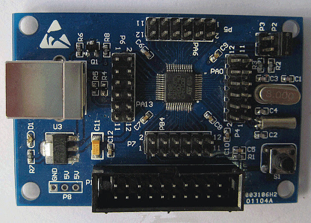
To solve the layout problem, I bit the bullet and re-laid out everything on two boards – something I originally wanted to avoid to make for a slimmer case and bring the cost down. It took two whole days, but the readability of the layout greatly improved. Bonus: the boards were now small enough to be mounted behind a Eurorack panel – this mattered to me since I was starting building my little modular setup at that time.

The VCO problem was a tough one, because I spent a lot of energy trying to solve the wrong problem. My original focus was on the integrator reset time in the saw-core, but even by faking Spice models of the crappiest JFETs, or of op-amps with the most horrible offsets, or of comparators slow as molasses, I could not get in simulation something as bad as what I was measuring. That’s when I decided to pimp my measuring equipment and get something more serious to probe the integrator current source…


After a few days blocked on the problem, everything pointed to the exponential converter – something confirmed after rapidly breadboarding a standard transistor-pair expo converter in place of the 2164 and getting 5 octaves of tracking minus temperature stability. It took me a while to figure out what was wrong… It turned out that the SSM2164 input is not the ideal virtual ground I thought it was! The problem was solved by increasing the value of the resistor at the 2164 input (from 15k to 100k) – less current, less non-linearities affecting scaling.

With that problem fixed, I got a second proto made. The interface was much better, and the VCO tracked well over 5 octaves (the remaining error was due to the integrator reset time and some errors in the 2164 expo response – would have required more circuitry for compensation…).

What remained to be solved was what to put in place of the analog-style step sequencer. I quickly toyed with the idea of an 8 steps waveform editor for the LFO (a kind of sequencer but at modulation rates) – wasn’t good. I had 9 knobs, roughly 40% of the CPU after some optimizations, and 2 days left before a demo at Modular Square. And this is when I decided to ressucitate… eigendrums. This was a quite old drum machine concept inspired by an ISMIR paper by Ellis and Arroyo. Let’s do it!

First problem was how to get audio out of the MCU. Solved by hacking the board to hook up the MCU PWM pin to the output op-amp (I also tried hooking it into the VCF->VCA, but then it sucked because a synth note had to be played for the drums to be heard). I had to swap the functions of two MCUs pins for that. Damn, the Shruthi-1 made me sick of PWM and I was at it again…


Second problem was to code a drumsynth with a very low CPU requirement. Simplest approach that could work: a digital sine oscillator with AD envelope for pitch and amplitude + noise + ringmod. Since I decided to dedicate only one knob for adjusting the tone, the knob worked as a morphing control through various combination of parameters that I programmed into the unit through CC with a MIDIpal, writing down parameter values on paper. Later I ditched the ringmod and used a sample for the HH.


Third problem was the drum pattern generation. I wanted something fun to play with, that could generate musically interesting patterns, and that could allow the classic “build-ups” found in electronic music. My first try, the straightforward eigenrhythm implementation worked well, but it was not fun to play. At this stage, I had 6 knobs controlling the 6 principal components + 3 for tone control. The problem was that the last knobs had decreasing impact (PCA “sorts” dimensions by decreasing variance), and that there was no way of getting dense or sparse patterns – the PCA learned the “average” density of a pattern and I wanted a way of bringing in outliers too! What I wanted was something more like an euclidean sequencer, in which it is possible to control sparsity/density. So let us work backwards… With 3 knobs dedicated to a sparsity/density control for each instrument (how would it work? TBD…), this would leave me with only 2 knobs for controlling the base structure of the drum pattern. How to map the space of drum patterns into a 2D space? My first approach was to get a bank of presets, lay them out in 2D using the first 2 axes of the PCA, and use the 2 knobs as X/Y coordinates in this space (did it before, see figure 4). Problem: the map has gaps, and I don’t want to store many patterns in flash. Same problem with LLE. I want hmmm… something like a topology-aware VQ that would give me a grid-like codebook? How is that called? Kohonen map! That’s how I decided to use self-organizing maps to build a 2D grid of patterns. Last open problem was the sparsity/density control – once you have a pattern, how to progressively remove notes to turn it into an empty pattern, and how to progressively add notes to turn it into a grid of sixteenth notes. If, like me, your past job involved counting n-grams and solving combinatorial optimization problems, the solution gets very obvious: select the sequence of note addition/removals that visits the rhythmic patterns with the highest frequency in a corpus of drum loops. The library is the grammar. Nice side-effect: randomly walking through this Hamming neighborhood creates musically interesting variations for free! I made it in time for the Modular Square demo – though the whole thing was trained in a small corpus of rhythms (larger model on its way – it did not make it into the first version of the Anushri firmware).

After the Modular Square demo, I noticed something odd about my proto… When switching from the single board layout to the 2 boards layout, I blindly rearranged the available controls without realizing there was room for more! I added two knobs, changing the number of software knobs from 9 to 10 (functions: VCO detune, velocity destination control, and a bitcrusher for the drum section which is the FX maximizing the wow/CPU cycles ratio – leaving all competitors in the dust); and adding a knob for sub-oscillator level. And more room for 2 modular I/O jacks! This is how we got to the present third revision of the board.

The final touches to the firmware included a secret way of overriding the drum sequencer with a x0x pattern input on the keyboard, a way of sequencing the drum section from an external source, and bringing back the CC drum sounds editing I used during development.

All in all, the project took 1 month of hardcore development to get the basics done, 3 months to feel “right”, and 4 months of polishing – which are the ratios I am getting used to!

4/02/2013

STM32F103C8T6 Performance line, ARM-based 32-bit MCU with Flash, USB, CAN, seven 16-bit timers, two ADCs and nine communication interfaces


The STM32F103C8T6 performance line family incorporates the high-performance ARM Cortex-M3 32-bit RISC core operating at a 72 MHz frequency, high-speed embedded memories (Flash memory up to 128Kbytes and SRAM up to 20 Kbytes), and an extensive range of enhanced I/Os and peripherals connected to two APB buses. All devices offer two 12-bit ADCs, three general purpose 16-bit timers plus one PWM timer, as well as standard and advanced communication interfaces: up to two I2Cs and SPIs, three USARTs, an USB and a CAN.

The STM32F103C8T6 performance line family operates in the −40 to +105 °C temperature range, from a 2.0 to 3.6 V power supply. A comprehensive set of power-saving mode allows to design low-power applications.

The complete STM32F103xx performance line family includes devices in 4 different package types: from 48 pins to 100 pins. Depending on the device chosen, different sets of peripherals are included, the description below gives an overview of the complete range of peripherals proposed in this family.

4/01/2013

TDA7000 FM Receiver / TV Tuner


TDA7000 is a great chip because it includes RF input stage, mixer, local oscillator, IF (intermediate frequency) Limiter, IF filter, amplifier, Phase demodulator, Mute detector, Frequency-Locked-Loop system and voltage controlled oscillator (VCO) all in a single chip, so you don't have to do so much tuning and tweaking as you would normally do in super heterodyne receivers. TDA7000 is also a great choice for folks that don't have great experience with RF circuits due to the fact that there are few external capacitors & resistors needed, no external IF filters, and only one variable coil and varicap diode.

The IC has an FLL (Frequency-Locked-Loop) system with an intermediate frequency of 70 kHz. The IF selectivity is obtained by active RC filters. The only function which needs alignment is the resonant circuit for the oscillator, thus selecting the reception frequency.


Spurious reception is avoided by means of using a muting circuit similar to squelch. This eliminates and rejects other input signals around selected frequency so that even remote stations can sound clear just as if they were located near by.